
NewsQuality & Process
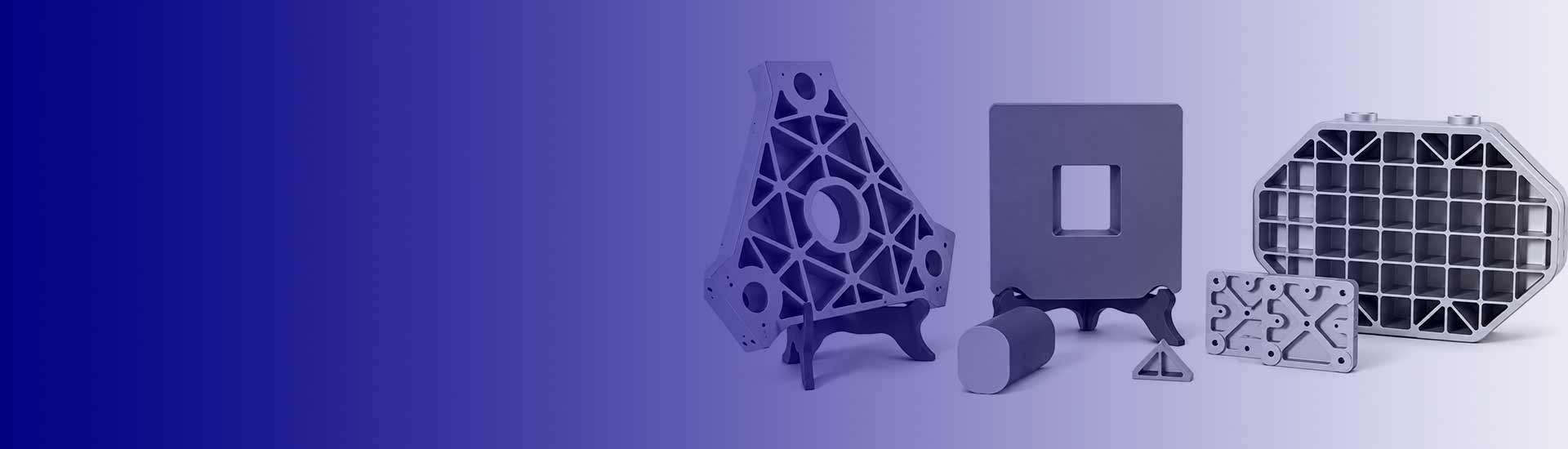
Silicon carbide (SiC) ceramics are among the most widely used advanced engineering ceramics, known for their exceptional hardness, high thermal conductivity, excellent wear resistance, and outstanding chemical stability. making them widely applicable in fields including semiconductors, precision machinery, and optics.
However, its performance depends significantly on the manufacturing method, material composition, microstructure, and subsequent machining processes.
Different manufacturing routes, including reaction bonding, pressureless sintering, and hot pressing, produce silicon carbide ceramics with different characteristics.
This guide explores the fundamental properties, manufacturing methods, material classifications, precision machining techniques, and industrial applications of silicon carbide ceramics. It also provides practical considerations for selecting materials and evaluating custom silicon carbide ceramic manufacturers.
Silicon carbide (SiC) is an advanced ceramic material composed of silicon and carbon atoms bonded through strong covalent bonds. Its unique crystal structure gives it a combination of high hardness, excellent thermal conductivity, low thermal expansion, and outstanding chemical resistance.
Silicon carbide (SiC) exhibits exceptional hardness, making it highly resistant to abrasive wear and surface damage.
Mohs Hardness: Approximately 9–9.5, indicating excellent scratch resistance.
Vickers Hardness: Approximately 26 GPa (2650 HV0.5), demonstrating its high resistance to indentation and localized deformation.
Prepared through specialized forming and sintering processes, it can achieve the density, mechanical strength, and microstructure required for demanding applications.
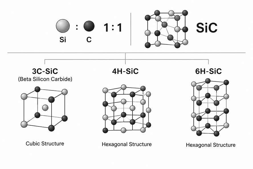
Silicon carbide has a chemical formula of SiC, with a theoretical silicon-to-carbon atomic ratio of 1:1.It exists in different crystalline structures known as polytypes, primarily distinguished by their atomic stacking sequences.
The most common polytypes include:
3C-SiC (Beta Silicon Carbide): A cubic crystal structure.
4H-SiC: A hexagonal crystal structure widely used in power semiconductor applications.
6H-SiC: Another hexagonal structure commonly found in silicon carbide materials.
The crystal structure and grain characteristics influence the material’s mechanical, thermal, and electrical properties.
Although both materials are based on SiC, structural silicon carbide ceramics and semiconductor-grade silicon carbide serve different purposes.
| Characteristic | Structural SiC Ceramic | Semiconductor SiC |
|---|---|---|
| Material structure | Polycrystalline | Single crystal |
| Main purpose | Structural and functional components | Electronic devices |
| Manufacturing | Forming and sintering | Crystal growth |
| Key properties | Hardness, wear resistance, thermal stability | Semiconductor performance |
| Typical applications | Mechanical seals, vacuum chucks, optical structures | Power MOSFETs, diodes, electronic devices |
Silicon carbide ceramics can be classified based on the processes used to produce them; these processes result in variations in density, mechanical properties, and machining characteristics.
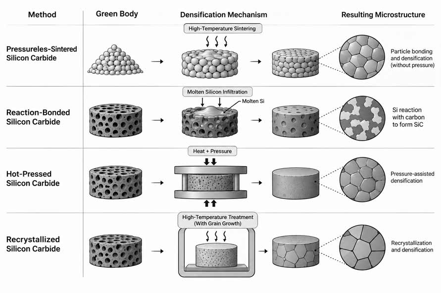
Common types currently in use include: reaction-bonded silicon carbide, pressureless-sintered silicon carbide, hot-pressed silicon carbide, and recrystallized silicon carbide.
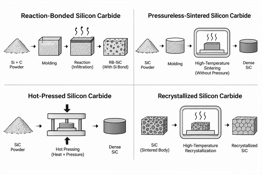
Reaction-bonded silicon carbide, also known as silicon-infiltrated silicon carbide (SiSiC), is manufactured by infiltrating a porous carbon-containing preform with molten silicon.
During infiltration, silicon reacts with carbon to form additional silicon carbide, while some residual free silicon may remain within the material structure.
Silicon carbide produced via this process is highly suitable for manufacturing large components with complex structures.
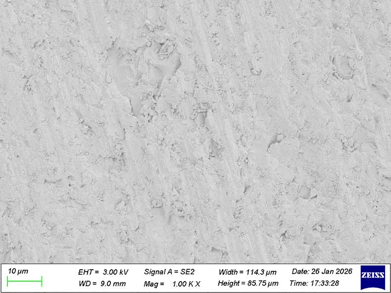
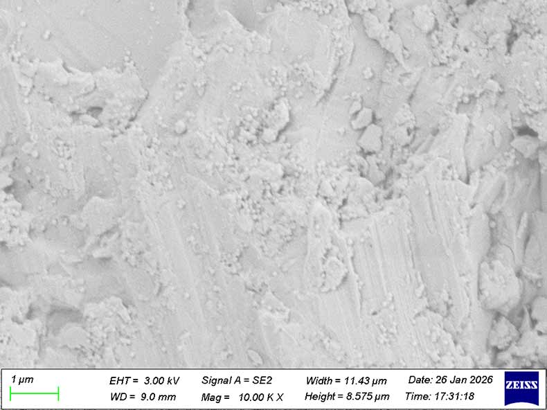
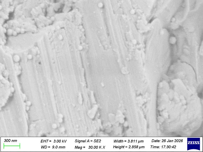
Figure 1. Representative SEM microstructure of reaction-bonded silicon carbide.
Pressureless-sintered silicon carbide is produced by consolidating fine silicon carbide powder at high temperatures without applying external mechanical pressure.Sintering additives are commonly introduced to facilitate densification and control the resulting microstructure.
This process can be used to produce anti-static or conductive-grade silicon carbide to meet industrial requirements.
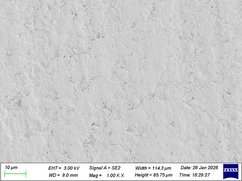
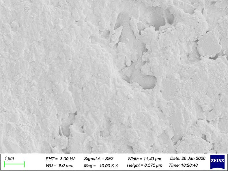
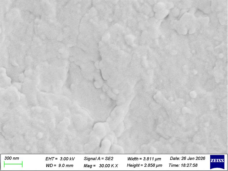
Figure 2. Representative SEM microstructure of pressureless-sintered silicon carbide.
Hot-pressed silicon carbide is produced by applying high temperature and uniaxial mechanical pressure simultaneously during the sintering process.Silicon carbide manufactured via this method is highly dense and possesses extremely low porosity.
However, this process imposes stringent technical requirements on the manufacturer and entails high production costs, making it unsuitable for large-scale or mass production of components.
Hot isostatic pressing uses high temperature and uniformly applied gas pressure to improve material densification.Unlike conventional hot pressing, which applies pressure primarily along one direction, HIP applies pressure from multiple directions.
Silicon carbide that has undergone hot isostatic pressing is typically used in high-end industrial applications with extremely demanding requirements.
Recrystallized silicon carbide is produced by forming silicon carbide particles into a desired shape and heating them to high temperatures, allowing the particles to bond through recrystallization.Unlike fully dense sintered silicon carbide, recrystallized SiC generally retains a porous structure.
It is typically used in high-temperature applications, such as in kiln furniture or furnace internal components.
| Material Type | Manufacturing Method | Main Characteristics | Typical Applications |
|---|---|---|---|
| RBSC / SiSiC | Molten silicon infiltration | Good dimensional stability, residual silicon phase | Optical mirrors, precision structures |
| Pressureless-Sintered SiC | High-temperature sintering without external pressure | High hardness, strength, and chemical resistance | Semiconductor and mechanical components |
| Hot-Pressed SiC | High-temperature uniaxial pressing | High density and mechanical performance | Specialized high-performance parts |
| HIP-SiC | High-temperature isostatic gas pressing | Reduced residual porosity | Advanced engineering components |
| RSiC | High-temperature recrystallization | Porous structure, excellent thermal stability | Furnace and kiln components |
Silicon carbide has a Mohs hardness of approximately 9–9.5—second only to diamond—which is why it is frequently found in mechanical seals, pump components, and industrial nozzles.
Silicon carbide has a thermal conductivity of approximately 110 W/mK—second only to aluminum nitride—and is frequently used in many types of semiconductor equipment.
Silicon carbide has a relatively low coefficient of thermal expansion.
This helps reduce dimensional changes caused by temperature variations and makes it suitable for precision components operating under changing thermal conditions.
Silicon carbide can be used at temperatures up to 1600°C, while maintaining its performance and structural integrity even at such high temperatures.
Silicon carbide offers excellent resistance to many corrosive chemicals and industrial environments. However, it is not a universal solution; strong oxidizing agents, certain molten substances, and specific high-temperature chemical environments may cause the material’s performance to degrade.
The electrical properties of silicon carbide ceramics depend on their composition, additives, and manufacturing process.This flexibility allows silicon carbide to have its resistivity adjusted according to the requirements of specific applications.
The manufacturing of silicon carbide ceramics involves several stages, including powder preparation, forming, densification, and precision machining.
The powder characteristics of silicon carbide—including particle size distribution, purity, morphology, and chemical composition—all influence subsequent forming and sintering processes. For instance, in the pressureless sintering of SiC, appropriate sintering additives may be introduced to achieve densification; meanwhile, for reaction-bonded silicon carbide, the preparation process requires the use of carbon-containing preforms to facilitate silicon infiltration.
Once the powder has been prepared, it undergoes a forming process; common forming techniques include dry pressing, isostatic pressing, extrusion, and slip casting.
The forming process produces a green body that must undergo the appropriate thermal treatment.Different SiC manufacturing methods use different densification mechanisms.These differences ultimately lead to distinct microstructures, which affect the final properties of the material.
After densification, silicon carbide ceramic components often require additional machining to achieve their final dimensions and surface quality.Depending on the component design, machining operations may include surface grinding, cylindrical grinding, hole machining, slot machining, lapping, and polishing.
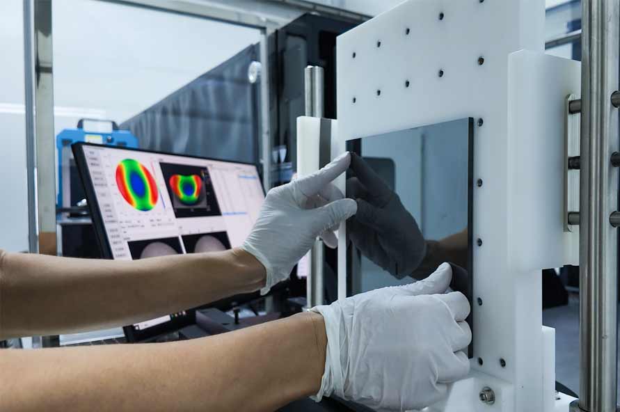
The final manufacturing stage involves dimensional inspection and surface quality verification. This typically entails checking parameters such as the dimensional accuracy, flatness, and parallelism of the parts. Depending on the specific requirements, measurements are performed using equipment such as coordinate measuring machines (CMMs), laser interferometers, and surface roughness testers.
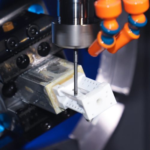
Silicon carbide has extremely high hardness. Achieving precision-machined components that meet demanding application requirements requires carefully selected cutting tools, machining processes, and inspection methods.
High tool wear
The high hardness of silicon carbide causes rapid abrasive wear of conventional machining tools. Diamond-based tooling is commonly used for grinding and machining SiC components.
Brittleness and edge chipping
Silicon carbide has limited fracture toughness compared with many metals. Excessive cutting forces or unsuitable machining parameters can cause edge chipping, microcracks, and local material breakage.
Different material microstructures
Reaction-bonded and pressureless-sintered SiC may exhibit different material-removal characteristics because of their different microstructures and compositions.
Complex geometries and tight tolerances
Thin walls, small holes, narrow slots, and complex internal structures require careful machining strategies to control deformation, fracture, and dimensional errors.
Diamond tooling is commonly used because of its high hardness and wear resistance.Depending on the operation and material grade, machining may use:
In Jundro’s machining experience, both sintered diamond and conventional electroplated diamond tools can be used for SiC machining.However, when machining small holes and narrow slots, conventional electroplated diamond tools tend to experience relatively high wear and may require more frequent replacement.
| Machining Process | Purpose | Typical Applications |
|---|---|---|
| Surface Grinding | Control thickness, flatness, and surface finish | Plates, substrates, chuck surfaces |
| Cylindrical Grinding | Machine external cylindrical surfaces | Sleeves, shafts, rings |
| CNC Machining | Produce complex geometries, holes, slots, and structural features | Housings, brackets, micro-hole components |
| Precision Lapping | Improve flatness and achieve high-precision surface geometry | Precision plates, reference surfaces, ceramic substrates |
| Precision Polishing | Reduce surface roughness and improve optical surface quality | Mirrors, optical components, precision reference surfaces |
The appropriate machining sequence depends on the material type and the final component requirements.
Electrical discharge machining can be considered for electrically conductive silicon carbide materials.For example, certain conductive reaction-bonded SiC grades can be processed using EDM for suitable hole and structural features.
However, EDM is not applicable to all silicon carbide ceramics. The material must have sufficient electrical conductivity
For long through-holes, EDM may provide an alternative to conventional diamond-tool machining when the material and component design are suitable.
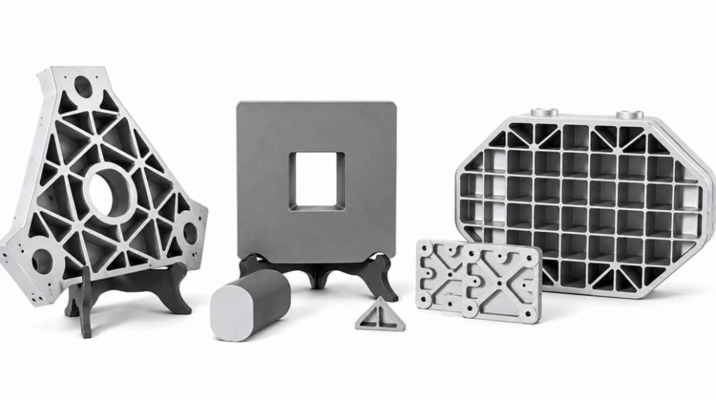
Lightweight silicon carbide components are often designed with internal cavities, ribs, pockets, or other material-reduction structures.For certain components, the general manufacturing approach is to produce the SiC blank first and then use CNC machining to create the required lightweight geometry.
Material quality: Material defects, cracks, and non-uniformity can affect machining stability.
Tool selection: Diamond tool type and condition influence tool life and surface quality.
Machining allowance: Excessive material removal can increase machining time and the risk of damage.
Component geometry: Thin walls, micro-holes, and narrow slots require careful process planning.
Inspection strategy: Critical dimensions and surface parameters should be verified using suitable measuring equipment.
Silicon carbide ceramics are used in industries where high hardness, wear resistance, thermal stability, and chemical resistance are essential.
Silicon carbide is not always the best material for every application. Depending on the operating environment, alumina and silicon nitride may offer more suitable combinations of cost, mechanical properties, and manufacturing characteristics.
Compared with alumina, silicon carbide offers higher thermal conductivity and wear resistance in many applications. However, if these enhanced properties are not necessary for your application, there is no need to pay the premium for SiC. Alumina is a more affordable and practical choice.
Silicon nitride (Si₃N₄) is known for its high fracture toughness, good thermal shock resistance, and mechanical strength.Compared with silicon nitride, silicon carbide generally offers lower fracture toughness and impact resistance, but better wear resistance and thermal conductivity.
| Properties | Alumina | Silicon Carbide | Silicon Nitride |
|---|---|---|---|
| Density (g/cm³) | 3.93 | 3.15 | 3.2 |
| Hardness (GPa) | 18 | 29 | 15 |
| Thermal Conductivity (W/m·K) | 30.8 | 110 | 25 |
| Fracture Toughness (MPa·m½) | 4.5 | 4 | 8 |
Standard material properties alone do not determine whether a silicon carbide component will perform successfully in an application. Component geometry, machining accuracy, surface quality, and inspection requirements are equally important.
Jundro focuses on high-precision, small-batch custom manufacturing of hard and brittle material components, including silicon carbide ceramics.
Rather than pursuing mass production, our work concentrates on complex structures, demanding tolerances, and specialized machining requirements.
| Parameter | Machining Capability |
|---|---|
| Maximum Workpiece Size | Ø450 mm |
| Flatness | 0.001 mm (Ø300 mm) |
| Concentricity | 0.005 mm |
| Cylindricity | 0.001 mm |
| Parallelism | 0.001 mm |
| Minimum Wall Thickness | 0.2 mm |
| Minimum Hole Diameter | 0.1 mm |
| Minimum Slot Width | 0.5 mm |
| Minimum Internal Thread | M1.6 |
| Polishing | Ra 0.005 µm |
| Sandblasting / Surface Roughening | Ra 2.0 µm |
Component: Silicon carbide mirror.
Surface roughness: Ra 0.02 μm.
Flatness: 0.003 mm.
Silicon carbide optical mirrors maintain excellent dimensional stability under temperature fluctuations. Their high thermal conductivity and low thermal expansion help minimize thermal deformation and preserve optical accuracy.
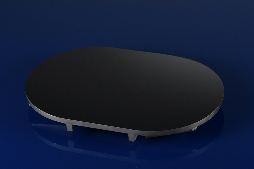
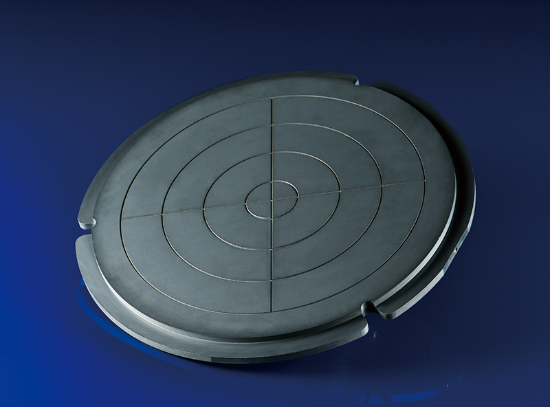
We manufacture precision silicon carbide ceramic chucks in various configurations, including pin-type, porous, vacuum, and custom-designed chucks.
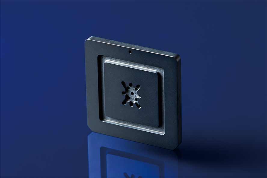
Precision machining of micro-holes as small as Ø0.1 mm in silicon carbide ceramics
Choosing the right silicon carbide manufacturer involves more than comparing material prices. It also requires evaluating material properties, machining experience, manufacturing capabilities, inspection equipment, and the ability to manufacture parts according to technical drawings.
Before placing an order, request a detailed Material Data Sheet from the supplier and verify that the specified properties meet your application requirements. Even within reaction-bonded silicon carbide (RB-SiC), differences in material composition and manufacturing processes can result in significant variations in density, hardness, thermal conductivity, and mechanical properties. Therefore, material selection should be based on verified specifications rather than the material name alone.
Silicon Carbide Datasheet from Jundro Ceramics:
Reaction-Sintered Silicon Carbide Data Sheet Download
Download Datasheet for Pressureless-Sintered Silicon Carbide
Not all ceramic machining suppliers have experience machining silicon carbide. Before working with a manufacturer, evaluate their previous machining projects and check whether their inspection equipment is complete. Without adequate inspection equipment, it is difficult to produce high-quality parts.
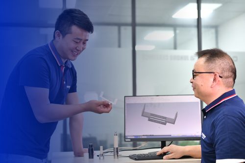
For custom SiC components, engineering communication is important before production.A capable manufacturer should review the drawings, identify potential machining challenges, evaluate tolerances, and clarify material and inspection requirements.
The appropriate supplier should be able to support the required production quantity and delivery schedule.For prototypes and small-batch components, engineering flexibility and process control may be more important than mass-production capacity.
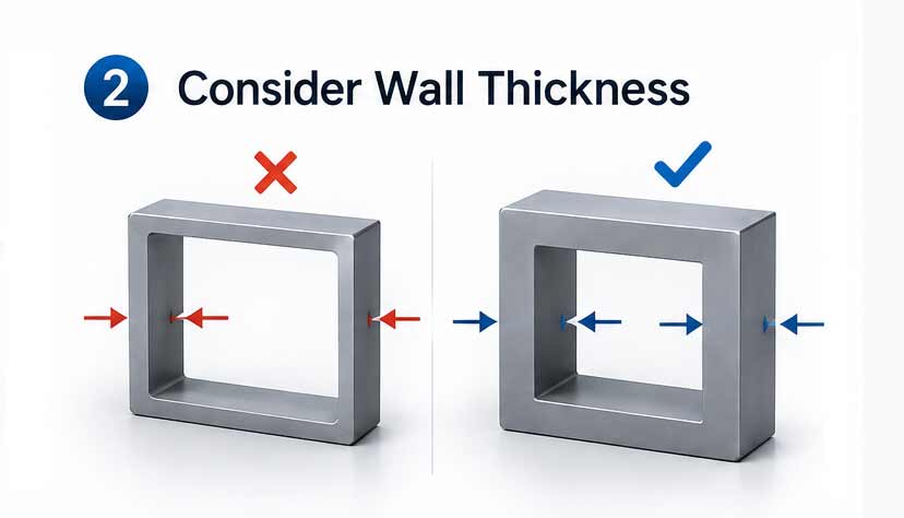
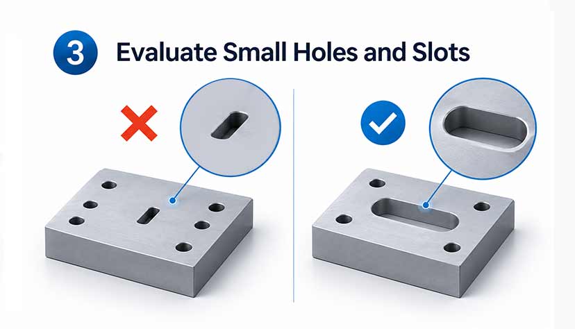
When initially designing silicon carbide components, please take into account the material’s inherent hardness and brittleness, and refer to the design recommendations we have provided to help you reduce unnecessary machining costs.
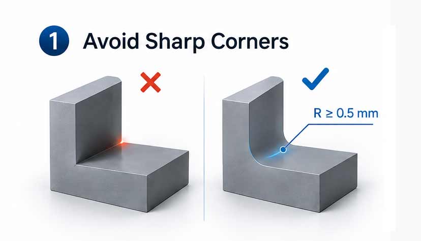
Internal sharp corners increase machining difficulty and cost, and can cause stress concentration that may lead to chipping or cracking. Where design requirements allow, use rounded corners whenever possible.
Thin walls and narrow geometric features are more sensitive to machining forces and brittle fracture. They are more likely to chip or crack during grinding or CNC milling, increasing material waste and the risk of part failure. As a result, manufacturers may include additional material costs in their quotations to account for potential machining losses.
Machining small holes and narrow slots often requires specialized tools and additional machining time, which increases the overall part cost.
Not every surface needs the same level of precision.
Clearly identify critical surfaces, flatness requirements, roughness values, and geometric tolerances. This helps avoid unnecessary polishing or precision machining.
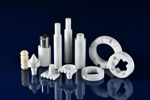
Silicon carbide ceramics are used in semiconductor equipment, precision optical systems, mechanical seals, pumps, wear-resistant components, and high-temperature industrial equipment. Their high hardness, thermal conductivity, and chemical stability make them suitable for demanding operating conditions.
Reaction-bonded SiC is produced by infiltrating a carbon-containing preform with molten silicon, which reacts with carbon to form additional silicon carbide. Some residual silicon may remain.
Pressureless-sintered SiC is produced by densifying SiC powder at high temperatures without external mechanical pressure, typically with the assistance of sintering additives.
The electrical properties of SiC ceramics depend on their composition, additives, and manufacturing process. Some grades are electrically conductive or anti-static, while others have different electrical characteristics.
Yes. Silicon carbide has extremely high hardness and is brittle, which makes it challenging to machine. Diamond-based tools are commonly used for grinding and precision machining. Tool wear, edge chipping, and dimensional control are important considerations.
Certain electrically conductive SiC grades can be processed using electrical discharge machining. However, EDM is not suitable for all silicon carbide ceramics. The material’s electrical conductivity and the required component geometry must be evaluated first.
Yes. Silicon carbide can be precision polished for optical and other high-quality surface applications. The achievable surface roughness and flatness depend on the material grade, component geometry, polishing process, and inspection method.
Not necessarily. Silicon carbide generally offers higher thermal conductivity and excellent wear resistance, while alumina is widely used for electrical insulation and cost-effective structural components.
To evaluate a custom SiC component, the manufacturer typically needs:
Providing complete technical information helps the manufacturer evaluate feasibility and prepare a more accurate quotation.
Jundro provides precision machining services for hard and brittle materials, including reaction-bonded and pressureless-sintered silicon carbide ceramics.Our focus is on small-batch custom components with complex geometries, demanding tolerances, and specialized machining requirements.
If you have a silicon carbide component drawing or a specific application requirement, contact our engineering and sales team for a manufacturing feasibility review.
Send us your drawings to discuss your custom silicon carbide ceramic project.

Chinese (Simplified)

English

German

Japanese

Spanish
Floors 1-2, Building 3, Qianyuan Industrial Park, No. 2 Gaoxin 2nd Road, Dalang Town, Dongguan, Guangdong, China(523770)